




L'équipe GenesInk
About L'équipe GenesInk
Posts by genesink :
Call for Projects « PERFECTO »: GenesInk winner for its « EcoZinc » project (eco-design of zinc oxide nanoparticles ZnO)
Electronics is one of the industrial sectors with the greatest impact on the environment in terms of CO2 emissions and waste. Since 2020, the government « France Relance » plan has been providing unprecedented and necessary financial support to SMEs committed to ecological transition and the drastic slowdown of current climate change.
Thanks to this plan, entrepreneurs and SMEs are immediately entering the “green economy” market (repackaging, eco-design and / or renewable energy) and large companies are reinventing themselves by changing their traditional models.
GenesInk is one of these dynamic SMEs committed to environmental and eco-design themes. Since mid-September 2021, this commitment has been rewarded following the response to the “Perfecto” call for projects aimed at implementing an eco-design approach based on Life Cycle analysis (LCA) one of the R&D processes aimed at marketing a product, process or service with high environmental performance.
GenesInk will take up this ambitious challenge by being one of the 15 winning companies among 42 projects submitted. Thus, this financial support will allow us to benefit from personalized support provided by ADEME (Environment and Energy Management Agency) in the establishment of a new process for synthesizing eco-designed zinc oxide (ZnO) nanoparticles (Illustration 1).
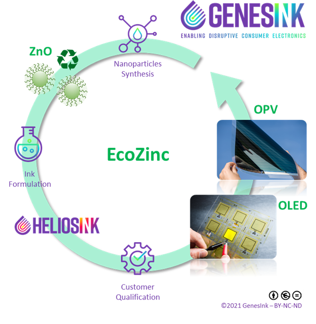 Illustration 1 – Eco-design process for synthesizing zinc oxide nanoparticles (ZnO) as part of the « EcoZinc » project
Preliminary studies based on the LCA of this new process were carried out in close collaboration with Ms. Chrystel Simone, LCA expert, and have enabled us to demonstrate a strong potential for reducing environmental impacts on all significant indicators, including a reduction more than 30% on 6 of the 9 indicators studied (Illustration 2) (climate change, human toxicity, particulate matter, acidification, freshwater eutrophication and ecotoxicity, resources depletion).
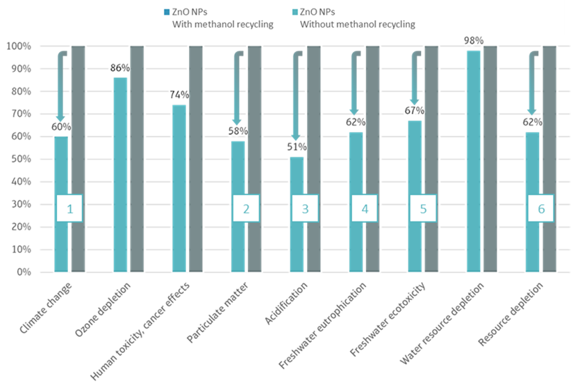 Illustration 2 – Comparative study of the environmental effects of the synthesis of nanoparticles (NPs) with and without methanol (MeOH) recycling
These eco-designed semiconductor inks are used by additive manufacturing methods for eco-technology applications such as OPV (Organic PhotoVoltaic) using solar energy for electricity production or OLED screens (Organic Light-Emitting Diodes) (Illustration 3).
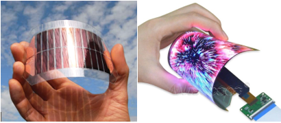
Illustration 3 – OPV technology (left) and OLED technology (right)
References:
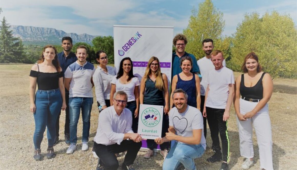
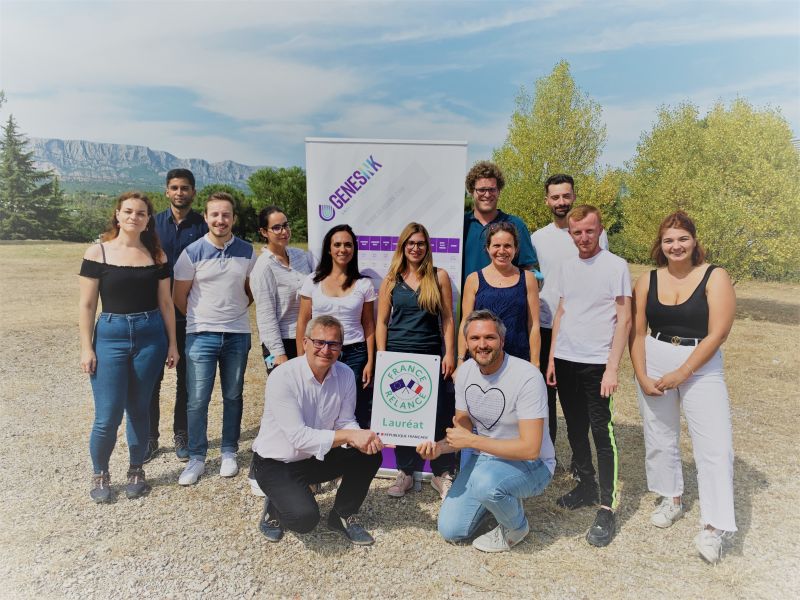
Thank you to the Ministère de l’Économie, des Finances et de la Relance and to Bpifrance
A lot of work, but just one word: #Proud. The best is yet to come.

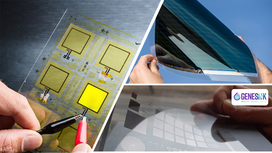
Are you looking for a highly innovative SME to build your future Research, Development, and Innovation projects?
GenesInk develops conductive and semi-conductive inks to enable new functionalities such as transparency, flexibility, and stretchability for the consumer electronics market. What makes GenesInk unique is its capability to solve technological issues such as reduce form factor, increase the tracks finesse and electrical performance resulting in highly functional, lightweight, and aesthetic electronic devices.
GenesInk is looking to integrate new European consortia to implement its nanoinks into energy generation and storage applications. we propose to offer our know-how and expertise in the conception of main nanomaterials for the different layers in PV (HTL, ETL, transparent electrode and top electrode). GenesInk is also aiming to develop new Ag nanoinks compatible with silicon-based photovoltaics.
If our expertise is of interest for you and you have a project idea in mind do not hesitate to contact our R&I team with high expertise in European proposals preparation and projects management: vanessa.douet@genesink.com; benjamin.dhuiege@genesink.com ; rita.faddoul@genesink.com.

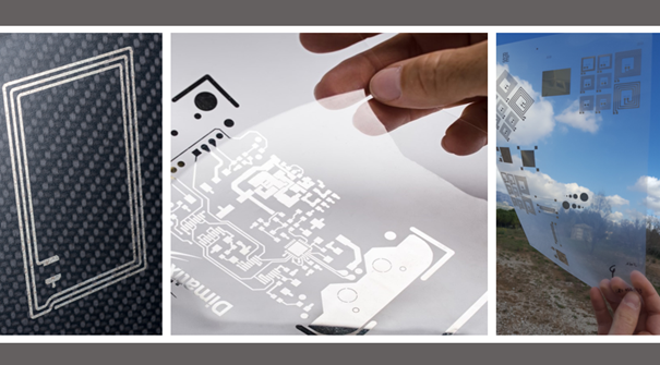
Are you looking for a highly innovative SME to build your future Research, Development, and Innovation projects ?
GenesInk develops conductive and semi-conductive inks to enable new functionalities such as transparency, flexibility, and stretchability for the consumer electronics market. What makes GenesInk unique is its capability to solve technological issues such as reduce form factor, increase the tracks finesse and electrical performance resulting in highly functional, lightweight, and aesthetic electronic devices.
GenesInk is looking to integrate new European consortia to implement its nanoinks into 5G and integrated antennas in connected objects.
If our expertise is of interest for you and you have a project idea in mind do not hesitate to contact our R&I team with high expertise in European proposals preparation and management : vanessa.douet@genesink.com; benjamin.dhuiege@genesink.com ; rita.faddoul@genesink.com.

European consortium to test new materials and manufacturing processes for consumer electronics


- The research is part of the European MADRAS project which will enable mass production of this type of electronics, known as OLAE, for accelerated time-to-market.
- Seen as a viable alternative to conventional electronics, OLAE devices include organic electronics printed on flexible surfaces such as plastic or paper.
- Their applications range from producing smart packaging, roll-up displays and flexible solar cells to single-use diagnostic devices and printed batteries along with other innovations.
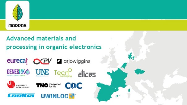
France, October 8th 2020.- The European MADRAS project aims to develop new materials and manufacturing processes for scalable mass production of organic electronics devices, also known as OLAE devices, integrated into plastic parts for accelerated time-to-market.
Progress in printed electronics and materials has paved the way for products with new features, lighter, thinner and more flexible. This has driven the development of the technology and the spread of applications for a range of sectors.
Organic devices are seen as a viable alternative to conventional inorganic conductors, such as copper and silicon. Their operation integrates organic electronics printed on flexible surfaces such as plastics or paper for numerous applications, including producing smart packaging, roll-up displays, flexible solar cells, single-use diagnostic devices and printed batteries along with other innovations.
In the words of Rosa Araujo, a project manager at Eurecat and MADRAS coordinator, MADRAS aims to “demonstrate an improvement in OLAE devices by establishing a robust alternative manufacturing methodology and an innovative approach in a scalable competitive process.”
The project “proposes two products for the people authentication market and smart manufacturing, which will showcase a shift towards digitisation and the Internet of Things so as to contribute to the sustainable deployment of smart products for consumer use,” she notes. These products “belong to the global emerging trend of structural electronics with very large addressable markets such as the automotive industry, healthcare and many others.”
In the MADRAS project “we will work on developing transparent conductive materials which will allow for building stable printed devices with longer lifetimes,” points out Eugenia Martínez-Ferrero, the project’s technical coordinator and head of the Photonics line in Eurecat’s Functional Printing and Integrated Systems Unit. “These new features will make it possible to make more exciting and lower-cost integrated products.”
The MADRAS project will use In-Mould Electronics, also known as plastronics, to enhance the device integration process, increasing resistance to humidity and wear and tear and adding custom-made connectors, and additionally as a manufacturing process for the advanced materials with better conductive and resistant properties proposed in the project. This technology combines functional printing of electronics and hybridisation of electronic components with traditional plastic transformation processes, such as thermoforming and injection, to create plastic parts with electronic functions.
The innovative technology developed as part of the project will be implemented in two printed electronics demonstrators integrated into plastic parts. Specifically, it will be demonstrated with a flexible geolocation label for the packaging sector and a biometric photosensor which will be employed to identify users of an electric mobility service.
The MADRAS project is funded by the European Union’s Horizon 2020 programme and coordinated by the Eurecat technology centre. It involves 11 other partners from Spain (Eticas Research and Consulting, TECNOPACKAGING, UNE and the Cooltra Group), France (GenesInk, Arjowiggins and Uwinloc), Denmark (infinityPV), the Netherlands (TNO) and the Czech Republic (COC and University of Pardubice).

Energy conversion / Energy generation
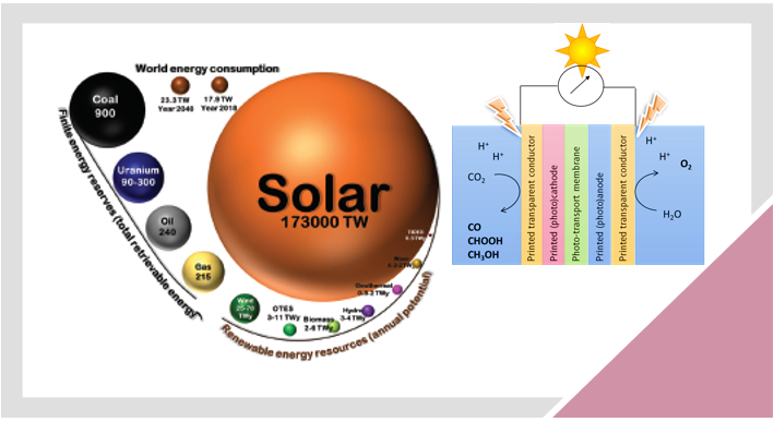
With the increasing European demand for renewable and greener energies, GenesInk develops conductive and semi-conductive nanoinks sustainably for you to create devices of tomorrow and meet the energies market demand (solar power and CO2 conversion, energy and batteries).
Our portfolio encompasses nanomaterials for electron and hole transport layers (ZnO, WOx, NiOx), transparent conductive electrodes (based on Ag nanowires) as well as catalysers for anodes and cathodes in energy conversion devices (Ag, Cu, ZnO, MgO). GenesInk provides know-how and expertise from synthesis, formulation, and industrialization processes on several printing methods and onto flexible and/or transparent substrates.
WEBINAR : SMART PACKAGING GENESINK'S SOLUTION TO MANY NEEDS

GenesInk reminds you the next webinar on “Smart packaging: GenesInk’s solution to many needs ”.
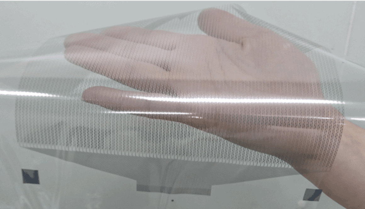
This webinar will give you more information and details on our range dedicated to smart and active packaging with conductive (antennas/sensors) and semi-conductive (OLEDs) nanoinks adapted for paper, polymer, and glass substrates.
Register and get to know our inks dedicated to smart packaging and electronics on papers.
Date : September 07,2020
Duration : 30min
Available sessions – click the link to register :
Contact information :
- Rahul ASHOK
Email: rahul.ashok@genesink.com
- Rita FADDOUL
Email: rita.faddoul@genesink.com

Smart integrated antennas technology for Aeronautics and Defence application
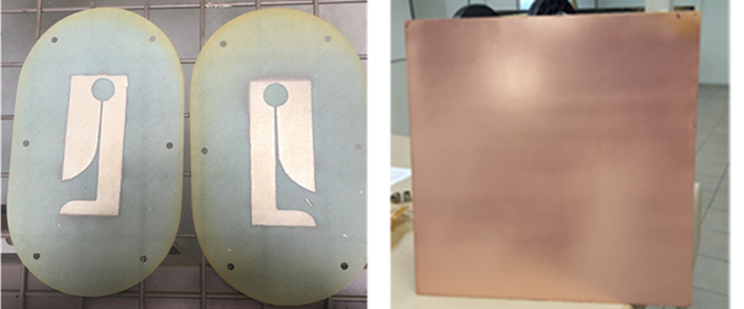
GenesInk develops conductive and semi-conductive nanoinks sustainably for aeronautics application. Our nanoinks allow you to create smart integrated antennas on composite and polymer materials by spray coating and printing techniques. Our technology has an excellent adhesion and conductivity on both rough and smooth surface with high radio performance in relevant environment (TRL 5-6). We can further optimize our nanoinks with your own specifications as well as develop novel nanoinks dedicated to your applications:
- Nanoinks based on Ag nanoparticles and flakes for integrated printed electronic devices (e.g. antennas, sensors, etc.). Thickness up to 40 µm if required.
- Innovative process of electroless, eco-friendly and cost-effective Cu metallization on polymer substrate as lightening protection systems.
- Nanoinks based on Ag nanoparticles and nanowires for Electro-Magnetic Interference Shielding and stealth applications.”
GenesInk recrute : Technicien Chimiste H/F
Description du poste et missions
Acteur de référence dans la conception et la formulation d’encres de spécialité, notre société GenesInk basée à Rousset (Bouches-du-Rhône) recherche un technicien chimiste H/F pour assurer la mise en œuvre, la conception, la formulation et le développement industriel de ses nouveaux produits.
Affecté(e) au département R&D, sous la responsabilité du Responsable Recherche et Développement, vous serez dans un premier temps en charge de la réalisation des travaux de conception des encres à l’échelle laboratoire et du développement de ces encres, notamment de l’optimisation des différents procédés à l’échelle laboratoire. Dans un second temps, vous assurerez l’industrialisation puis la production des encres à l’échelle pilote dans une démarche d’amélioration continue des performances. Le technicien de formulation doit avoir le sens de l’observation, être créatif, organisé et avoir le goût du travail en équipe.
Missions principales
Recherche :
- Mettre en œuvre des techniques de synthèse et caractériser les matières actives selon un cahier des charges ;
- Formuler les encres selon un cahier des charges précis ;
- Mettre en forme, interpréter et présenter les résultats expérimentaux ;
- Effectuer un état d’avancement des différents projets et signaler les éventuelles difficultés rencontrées ;
- Assurer la gestion de la métrologie ;
- Contribuer à l’optimisation et/ou à l’amélioration du fonctionnement du Laboratoire : HSE, installations, organisation.
Développement :
- Optimiser les différents paramètres des procédés de synthèse et de formulation ;
- Assister et participer aux essais pilotes ;
- Réaliser les analyses nécessaires aux traitements des RQP (Réclamations Qualité Produit) ;
- Définir les méthodes de suivi qualité et assurer le suivi des fabrications ;
- Participer à la gestion des dérogations et des non-conformités ;
- Participer à la fabrication et caractérisation des produits pour envoie aux partenaires des projets.
Compétences
De formation Bac+2 / Bac+3 Chimie, vous justifiez idéalement d’une expérience réussie et significative de 1 à 3 ans sur un poste similaire ou sur un projet en phase pilote (stage ou alternance compris). Candidature débutant acceptée.
Qualités
- Esprit d’équipe et qualités relationnelles ;
- Rigueur et autonomie dans l’organisation de son travail ;
- Capacités d’analyse et de synthèse ;
- Capacités rédactionnelles ;
- Disponibilité́ ;
- Capacité à travailler dans un contexte multiculturel ;
- Langue(s) : Français et Anglais courants ;
- Maîtrise du Pack Office (Excel, PowerPoint, Word) et des technologies de l’information et de la communication.
Statut :
Date d’embauche : Octobre 2020
Type de contrat : CDD avec possibilité CDI
Rémunération : à définir selon profil
Lieu : Rousset (13), avec des déplacements réguliers à prévoir
Contact :
CV et lettre de motivation à envoyer à l’adresse suivante :
vanessa.douet@genesink.com